
Alchitry Au V2 FPGA Development Board (Xilinx Artix 7) - แท้จาก Sparkfun, USA


| รหัสสินค้า | FB10013 |
| หมวดหมู่ | FPGA + Programmer |
| ราคา | 5,895.00 บาท |
| สถานะสินค้า | พร้อมส่ง |
| จำนวน | ชิ้น |

รายละเอียดสินค้า
Description:
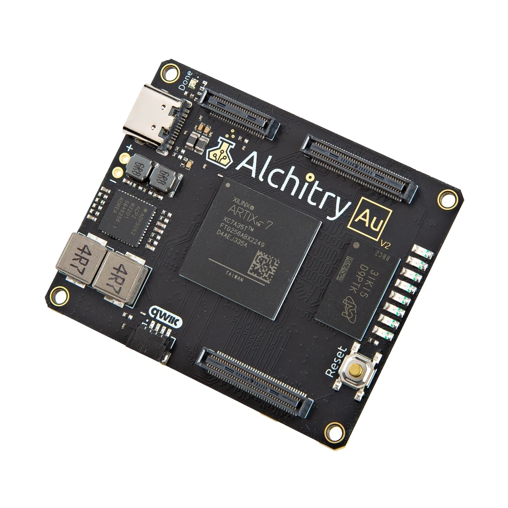
The Alchitry Au V2 is the "gold" standard for FPGA development boards and it's possibly one of the strongest boards of its type on the market. FPGAs, or Field-Programmable Gate Arrays, are an advanced development board type for engineers and hobbyists alike to experience the next step in programming with electronics. The Au continues the trend of more affordable and increasingly powerful FPGA boards arriving each year. This board is a fantastic starting point into the world of FPGAs and the heart of your next project.
The Artix 7 FPGA requires a free license for Vivado. Click here for instructions on installing it.
By adding stackable expansion boards similar to shields or HATs called "Elements," the Alchitry Au is able to expand its own hardware capabilities by adding prototyping spaces, buttons, LEDs, and more!
- XC7A35T-2FTG256I FPGA (speed and temperature grade upgrade over Au V1)
- 104 IO pins broken out across two headers
- 22 are triple voltage (3.3V, 2.5V, or 1.8V) of which 20 are LVDS_25 capable outputs
- 44 pins are routed as 100 ohm differential pairs (includes 20 dual voltage pins)
- Remaining IO routed as 50 ohm single ended (~90 ohm when used as diff pairs)
- 2 1.35V pins on bank B
- 8 pairs can be used as inputs to the XADC (0-1V input range)
- Remaining IO is at 3.3V
- All pairs can be used as LVDS_25 inputs except three pairs on bank B
- Control Header
- 8 IO pins also connected to on-board LEDs
- 1 IO pin also connected to on-board reset button
- JTAG
- Analog voltages and dedicated XADC input (0-1V range)
- Raw power input/3.3V regulated output
- QWIIC connector (shares pins on bank B)
- 100MHz oscillator
- 8 general purpose LEDs
- 1 button (typically used as reset)
- 256MB DDR3L @ 800Mb/s (400MHz)
- 32MBit Configuration FLASH
- FT2232HQ USB -> JTAG and USB -> UART (12Mbaud max)
- 5-12V input voltage on-board power supply
- 3.3V @ 4A (IO)
- 2.5V @ 500mA (tiple voltage pins, derived from 3.3V)
- 1V @ 4A (VCCINT)
- 1.8V @ 1.2A (VCCAUX, triple voltage pins)
- 1.35V @1.2A (DDR3L)
- 1.8V @ 200mA (analog)
- Schematic
- Drawing
- Pinout and Trace Lengths
- 3D Model (STEP)
- Simplified 3D Model (STEP)
- DC and AC Switching Characteristics (DS181)
- SelectIO Resources (UG471)
- Clocking Resources (UG472)
- All Xilinx Artix 7 Docs


วิธีการชำระเงิน
ชำระเงินค่าสินค้าโดยการโอนเงินเข้าบัญชีธนาคาร KBANK, SCB, BBL,TMB
กรุณาเก็บหลักฐานการโอนเงินของท่านไว้เพื่อแจ้งการชำระเงินด้วยค่ะ
ท่านสามารถแจ้งการชำระเงินผ่านระบบอัตโนมัติได้โดย Click Link ข้างล่างค่ะ
https://www.arduitronics.com/informpayment
ชำระเงินผ่านธนาคาร


@rfm0967y
ติดต่อสอบถาม
Join เป็นสมาชิกร้านค้า
MEMBER
