
A/D D/A Converter Module (PCF8591) แถมสายไฟ


| รหัสสินค้า | AG00041 |
| หมวดหมู่ | ADC / DAC Module |
| ราคา | 100.00 บาท |
| สถานะสินค้า | พร้อมส่ง |
| จำนวน | ชิ้น |
หยิบลงตะกร้า

รายละเอียดสินค้า
A/D D/A converter module (PCF8591)
โมดูล Analog to Digital และ Digital to Analog ขนาด 8 บิตนี้ จำนวน 4 Channel นี้ ทำงานโดยใช้ 8-bit successive approximation A/D conversion ซึ่งใช้ PCF8591
Module Specification
- Model: PCF8591
- Color: Blue + black
- Material: PCB + metal
- The PCF8591 is a single-chip, single-supply low power 8-bit CMOS data acquisition device with four analog inputs, one analog output and a serial I2C-bus interface
- Three address pins A0, A1 and A2 are used for programming the hardware address, allowing the use of up to eight devices connected to the I2C-bus without additional hardware
- Address, control and data to and from the device are transferred serially via the two-line bidirectional I2C-bus
- Single power supply
- Operating supply voltage 2.5 V to 6 V
- Low standby current
- Serial input/output via I2C-bus
- Address by 3 hardware address pins
- Sampling rate given by I2C-bus speed
- 4 analog inputs programmable as single-ended or differential inputs
- Auto-incremented channel selection
- Analog voltage range from VSS to VDD
- On-chip track and hold circuit
- 8-bit successive approximation A/D conversion
- Multiplying DAC with one analog output
Applications:
- Closed loop control systems
- Low power converter for remote data acquisition
- Battery operated equipment
- Acquisition of analog values in automotive, audio and TV applications
Packing list:
- 1 x A/D D/A converter module
- 4 x Dupont cables (21cm)
Dimensions: 1.57 in x 0.91 in x 0.39 in (4.0 cm x 2.3 cm x 1.0 cm)
Weight: 0.18 oz (5 g)
Weight: 0.18 oz (5 g)
PCF8591 IC Features
- Single power supply
- PCF8591 operating voltage range of 2.5V-6V
- Low standby current
- Via I2C bus serial input / output
- PCF8591 by 3 hardware address pins addressing
- PCF8591 I2C bus speed sampling rate decided
- 4 analog inputs programmable single-ended or differential input
- Automatic incremental channel selection
- PCF8591 analog voltage range from VSS to VDD
- PCF8591 built-in track-and-hold circuit
- 8-bit successive approximation A / D converter
- 1 analog output DAC gain
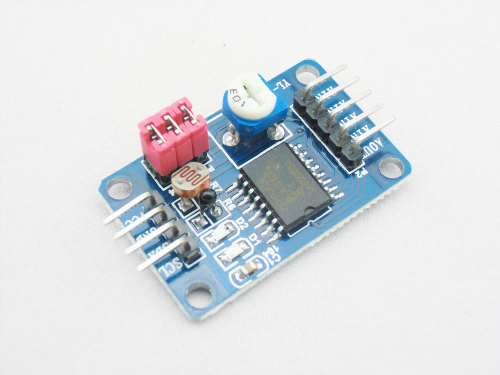
Module interface specification
The module on the left and right, respectively, to expand outside the 2-way pin header, respectively, as follows:
The left
- AOUT chip DA output interface
- AINO chip analog input interface 0
- AIN1 chip analog input interface 1
- AIN2 chip analog input interface 2
- AIN3 chip analog input interface 3
The right
- SCL – IIC clock interface connected to microcontroller IO port
- SDA – IIC digital interface connected to microcontroller IO port
- GND – connected to ground
- VCC – connected to 3.3v-5v
Four red jumper-cap instruction
- P4 – connected to P4 shorting cap, select thermistor access circuit
- P5 – connect P5 shorting cap, select photoresistor access circuit
- P6 – connected to P6 shorting cap, select 0-5V adjustable voltage access circuit
Documentation:
Tutorial
http://tronixstuff.com/2013/06/17/tutorial-arduino-and-pcf8591-adc-dac-ic/
วิธีการชำระเงิน
ชำระเงินค่าสินค้าโดยการโอนเงินเข้าบัญชีธนาคาร KBANK, SCB, BBL,TMB
กรุณาเก็บหลักฐานการโอนเงินของท่านไว้เพื่อแจ้งการชำระเงินด้วยค่ะ
ท่านสามารถแจ้งการชำระเงินผ่านระบบอัตโนมัติได้โดย Click Link ข้างล่างค่ะ
https://www.arduitronics.com/informpayment
ชำระเงินผ่านธนาคาร


@rfm0967y
ติดต่อสอบถาม
Join เป็นสมาชิกร้านค้า
ร้านArduitronics
/www.arduitronics.com/
สมัครสมาชิกร้านนี้ เพื่อรับสิทธิพิเศษ
MEMBER
สินค้าในตะกร้า ({{total_num}} รายการ)

ขออภัย ขณะนี้ยังไม่มีสินค้าในตะกร้า
ราคาสินค้าทั้งหมด
฿ {{price_format(total_price)}}
- ฿ {{price_format(discount.price)}}
ราคาสินค้าทั้งหมด
{{total_quantity}} ชิ้น
฿ {{price_format(after_product_price)}}
ราคาไม่รวมค่าจัดส่ง
➜ เลือกซื้อสินค้าเพิ่ม